Surface Modification Of Sensors And Microfluidics
The AIT Austrian Institute of Technology specializes in providing tailored services for the development of (bio)inks and surface modification of sensors and microfluidics. Our goal is to assist customers during the developmental stages of IVD (In Vitro Diagnostics) tests and sensing devices.
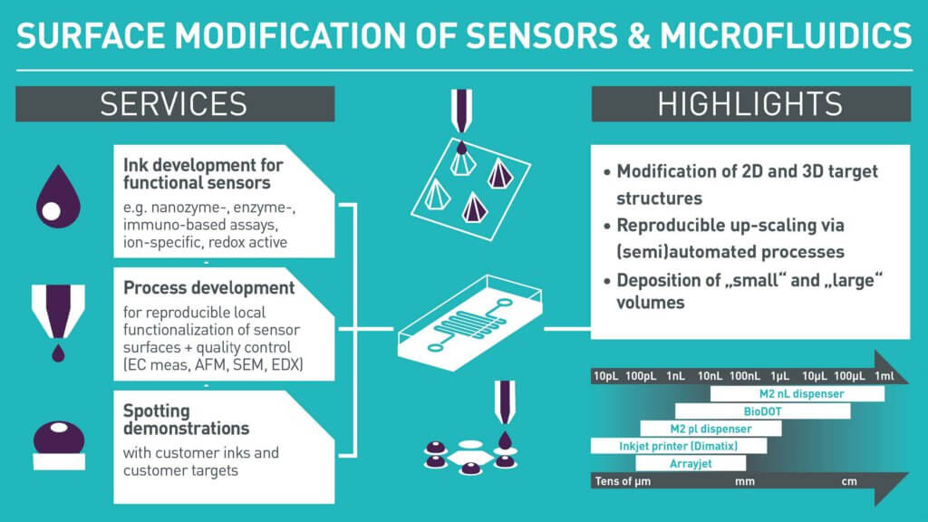
Within our well-equipped laboratories, we utilize state-of-the-art processing and analytical tools, specifically designed for small batch fabrication and rigorous process quality control. Our expertise extends to (bio)ink formulation, assay development, and the combination of chemical surface modification with advanced non-contact printing and dispensing techniques, applicable to both 2D and 3D target structures ranging from micrometers to centimeters in scale.
At AIT, we are committed to addressing your unique challenges by offering comprehensive support and employing appropriate methods and processes. Your success in overcoming obstacles is our priority, and we look forward to collaborating with you on your innovative projects.
Surface Modification Techniques
- Pico- and nanoliter dispensing on up to A3 substrates in a single run under controlled atmosphere (M2 i-One600, BioDOT AD1520)
- Precise inkjet printing on flexible substrates (Fujifilm Dimatix Material Printer DMP-2800)
- Microarray fabrication on solid support (e.g. gold, glass, …)
- Line dispensing (e.g. lateral flow device fabrication)
- Surface pretreatment using plasma activation, resin spin coating, wet chemical methods (e.g. modification, or activation)
Methods For Bioink Formulation
- Drop shape analyzer from Kruess (surface wetting properties, contact angle, surface free energy, and surface tension)
- Viscosimetry
- UV/VIS spectroscopy
- FTIR spectroscopy (ATR, transmission)
Methods For Process Quality Control
- Electrochemical measurement setups for amperometric (e.g. CV, CHA), impedance or potentiometric measurements
- Fluorescence scanner (TECAN, Agilent)
- Scanning electron microscope (SEM) with scanning transmission electron (STEM), back scattered electron (BSE) imaging and Energy Dispersive X-ray Microanalysis (EDX)
- Optical microscopy, surface profiler and AFM
Research Services
- Ink development for functional sensors, (bio)inks (e.g. nanozyme, enzyme, nucleic acids, immuno-based, ion-specific, redox active) and polymer/hydrogel inks for inkjet printing, spotting or line dispensing
- Process development for reproducible and scalable local functionalization of 2D and 3D structures (e.g. sensor sheets, microneedles, 96-well plates, semicondutor devices on wafer level) on the μm to cm-scale with pico- and nanoliter non-contact liquid handling techniques
- Fabrication of small batches (100-1000 pieces), processes can be run according to IVD ISO 13485
- Development of process quality control methods
- Quality control of surface modification in house by optical and electrochemical methods
- Spotting demonstrations with customers inks and customer targets
- Sensor characterization and support in development


